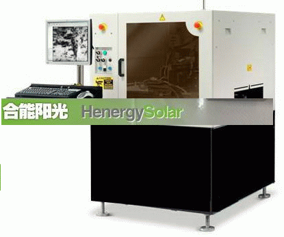
Photoluminescence (PL) Imaging is a unique non-invasive inspection tool as it can be used in-line at many different steps of the cell manufacturing process. This facilitates the direct comparison of data obtained at one process step to data obtained at another. Additionally, PL imaging can be compared to electroluminescence (EL) imaging on finished cells using comparable equipment.

Product's Feature
■Application:
■Mono crystal silicon wafers and cells,
■Poly crystal silicon wafers and cells
■Thin film cells
■Compounds cells
■Capabilities:
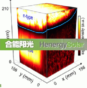
■Minority carrier lifetime scan
■ Silicon classification
■ Series resistance
■ Micro cracked
■ IV curve in dark and light conditions
■In-Line PL Imaging Benefits
■ Screen every wafer at in-line speeds
■Obtain information across entire wafer - not just at discrete points
■Identify Anomalous Cause Variations
■Identify and Track Defect Mitigation
■Define and Identify
■Responsible for low lowering yield and degrading efficiency
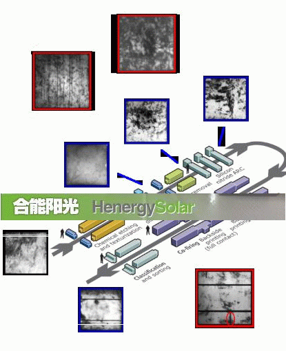
■Characterize wafers from processes steps.
■Measure and Analyze
■Obtain photoluminescence PL imagery of processing steps
■Track wafers through all processing steps
■Collate information for use in predictive model
■Tailored in-line design
■Improve and Control
■Integrate in-line equipment into production line
■Continuous improvement monitoring processes
■Used for electroluminescence imaging on finished cells
■ Only process good material
■Cost effectively improve throughput
■Maximize average cell efficiencies
■Tighten cell efficiency distribution
■Identify common and special cause variations in real-time
■We provide more than inspection equipment.
技术参数:
■ Indium gallium arsenide sensor :900-1500nm
■ Size: 23mm * 23mm ~ 200mm * 200mm
■ Pixels: 752 × 480pixel
■Testing time<1s
Typical Customer:
American,Europe and Asia and so on.